- 您现在的位置:买卖IC网 > Sheet目录2007 > MAX1113CPE+ (Maxim Integrated Products)IC ADC 8BIT LP 16-DIP
MAX1112/MAX1113
+5V, Low-Power, Multi-Channel,
Serial 8-Bit ADCs
2
_______________________________________________________________________________________
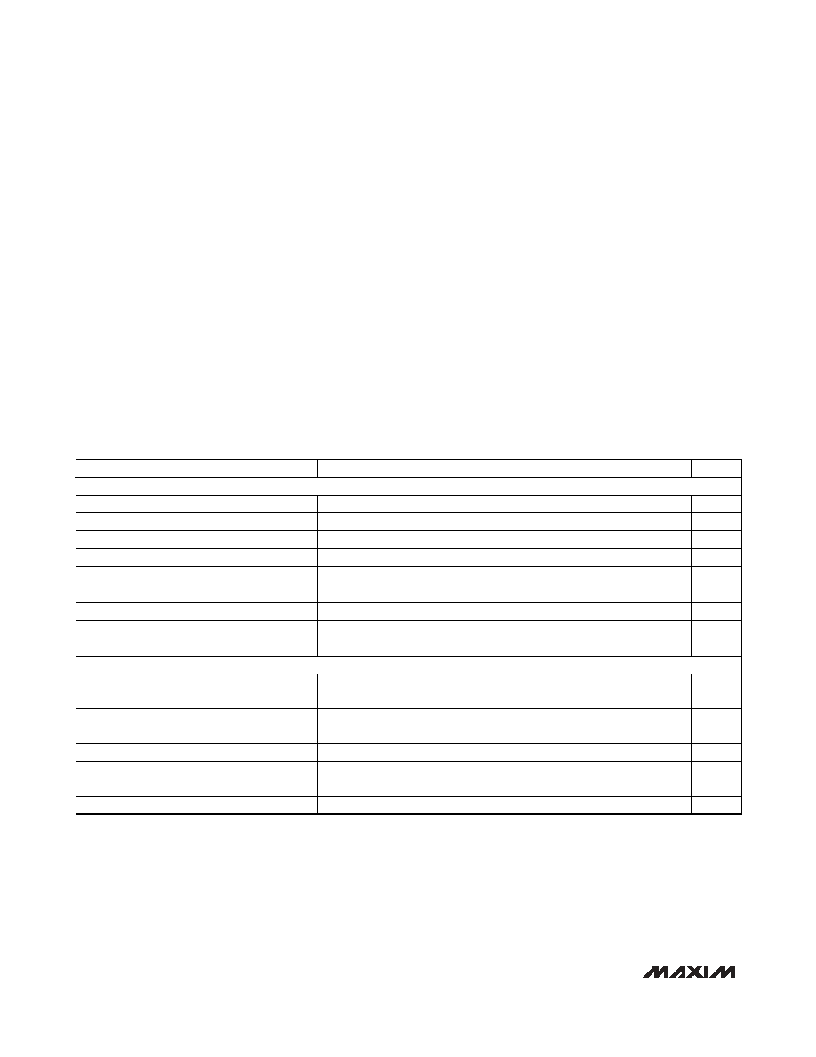
ABSOLUTE MAXIMUM RATINGS
Stresses beyond those listed under “Absolute Maximum Ratings” may cause permanent damage to the device. These are stress ratings only, and functional
operation of the device at these or any other conditions beyond those indicated in the operational sections of the specifications is not implied. Exposure to
absolute maximum rating conditions for extended periods may affect device reliability.
VDD to AGND............................................................-0.3V to +6V
AGND to DGND.....................................................-0.3V to +0.3V
CH0–CH7, COM, REFIN,
REFOUT to AGND ...................................-0.3V to (VDD + 0.3V)
Digital Inputs to DGND.............................................-0.3V to +6V
Digital Outputs to DGND ............................-0.3V to (VDD + 0.3V)
Continuous Power Dissipation (TA = +70°C)
QSOP (derate 8.30mW/°C above +70°C) .....................667mW
SSOP (derate 8.00mW/°C above +70°C) .....................640mW
Operating Temperature Ranges
MAX1112CAP/MAX1113CEE...............................0°C to +70°C
MAX1112EAP/MAX1113EEE ............................-40°C to +85°C
Storage Temperature Range .............................-65°C to +150°C
Lead Temperature (soldering, 10s) .................................+300°C
Soldering Temperature (reflow) .......................................+260°C
ELECTRICAL CHARACTERISTICS
(VDD = 4.5V to 5.5V; unipolar input mode; VCOM = 0V; fSCLK = 500kHz, external clock (50% duty cycle); 10 clocks/conversion cycle
(50ksps); 1F capacitor at REFOUT; TA = TMIN to TMAX; unless otherwise noted.)
-3dB rolloff
MHz
1.5
Small-Signal Bandwidth
kHz
800
VCH_ = 4.096VP-P, 25kHz (Note 3)
External reference, 4.096V
No missing codes over temperature
CONDITIONS
Full-Power Bandwidth
±1
Internal or external reference
LSB
Gain Error (Note 2)
dB
-75
Channel-to-Channel Crosstalk
dB
68
SFDR
Spurious-Free Dynamic Range
dB
-70
THD
Total Harmonic Distortion
(Up to the 5th Harmonic)
LSB
±0.1
Channel-to-Channel
Offset Matching
ppm/°C
±0.8
Gain Temperature Coefficient
LSB
±1
DNL
Differential Nonlinearity
UNITS
MIN
TYP
MAX
SYMBOL
PARAMETER
LSB
±0.3
±1
TUE
Total Unadjusted Error
Bits
8
Resolution
dB
49
SINAD
Signal-to-Noise
and Distortion Ratio
LSB
±0.1
±0.5
INL
Relative Accuracy (Note 1)
LSB
±0.3
±1
Offset Error
DC ACCURACY
DYNAMIC SPECIFICATIONS (10.034kHz sine-wave input, 4.096VP-P, 50ksps, 500kHz external clock)
发布紧急采购,3分钟左右您将得到回复。
相关PDF资料
MAX1116EKA+T
IC ADC 8BIT SERIAL SOT23-8
MAX11201BEUB+T
IC ADC 24BIT SRL 13.75SPS 10UMAX
MAX11202BEUB+T
IC ADC 24BIT SRL 13.75SPS 10UMAX
MAX11210EEE+T
ADC 24BIT 4WIRE SPI 16-QSOP
MAX11212BEUB+T
IC ADC 18BIT SRL 13.75SPS 10UMAX
MAX1135BCAP+
IC ADC 16BIT 150KSPS 20-SSOP
MAX1138LEEE+T
IC ADC 10BIT SERIAL 16-QSOP
MAX1159AEUI+
IC ADC 14BIT 135KSPS 28-TSSOP
相关代理商/技术参数
MAX1113EEE
功能描述:模数转换器 - ADC RoHS:否 制造商:Texas Instruments 通道数量:2 结构:Sigma-Delta 转换速率:125 SPs to 8 KSPs 分辨率:24 bit 输入类型:Differential 信噪比:107 dB 接口类型:SPI 工作电源电压:1.7 V to 3.6 V, 2.7 V to 5.25 V 最大工作温度:+ 85 C 安装风格:SMD/SMT 封装 / 箱体:VQFN-32
MAX1113EEE+
功能描述:模数转换器 - ADC 5V Low-Power Multi Ch Serial 8-Bit RoHS:否 制造商:Texas Instruments 通道数量:2 结构:Sigma-Delta 转换速率:125 SPs to 8 KSPs 分辨率:24 bit 输入类型:Differential 信噪比:107 dB 接口类型:SPI 工作电源电压:1.7 V to 3.6 V, 2.7 V to 5.25 V 最大工作温度:+ 85 C 安装风格:SMD/SMT 封装 / 箱体:VQFN-32
MAX1113EEE+T
功能描述:模数转换器 - ADC 5V Low-Power Multi Ch Serial 8-Bit RoHS:否 制造商:Texas Instruments 通道数量:2 结构:Sigma-Delta 转换速率:125 SPs to 8 KSPs 分辨率:24 bit 输入类型:Differential 信噪比:107 dB 接口类型:SPI 工作电源电压:1.7 V to 3.6 V, 2.7 V to 5.25 V 最大工作温度:+ 85 C 安装风格:SMD/SMT 封装 / 箱体:VQFN-32
MAX1113EEE-T
功能描述:模数转换器 - ADC RoHS:否 制造商:Texas Instruments 通道数量:2 结构:Sigma-Delta 转换速率:125 SPs to 8 KSPs 分辨率:24 bit 输入类型:Differential 信噪比:107 dB 接口类型:SPI 工作电源电压:1.7 V to 3.6 V, 2.7 V to 5.25 V 最大工作温度:+ 85 C 安装风格:SMD/SMT 封装 / 箱体:VQFN-32
MAX1113EPE
功能描述:模数转换器 - ADC RoHS:否 制造商:Texas Instruments 通道数量:2 结构:Sigma-Delta 转换速率:125 SPs to 8 KSPs 分辨率:24 bit 输入类型:Differential 信噪比:107 dB 接口类型:SPI 工作电源电压:1.7 V to 3.6 V, 2.7 V to 5.25 V 最大工作温度:+ 85 C 安装风格:SMD/SMT 封装 / 箱体:VQFN-32
MAX1113EPE+
功能描述:模数转换器 - ADC 5V Low-Power Multi Ch Serial 8-Bit RoHS:否 制造商:Texas Instruments 通道数量:2 结构:Sigma-Delta 转换速率:125 SPs to 8 KSPs 分辨率:24 bit 输入类型:Differential 信噪比:107 dB 接口类型:SPI 工作电源电压:1.7 V to 3.6 V, 2.7 V to 5.25 V 最大工作温度:+ 85 C 安装风格:SMD/SMT 封装 / 箱体:VQFN-32
MAX1113MJE
功能描述:模数转换器 - ADC
RoHS:否 制造商:Texas Instruments 通道数量:2 结构:Sigma-Delta 转换速率:125 SPs to 8 KSPs 分辨率:24 bit 输入类型:Differential 信噪比:107 dB 接口类型:SPI 工作电源电压:1.7 V to 3.6 V, 2.7 V to 5.25 V 最大工作温度:+ 85 C 安装风格:SMD/SMT 封装 / 箱体:VQFN-32
MAX1114
制造商:MAXIM 制造商全称:Maxim Integrated Products 功能描述:8-Bit, 150Msps Flash ADC